


광학,전자영상장비 (FE-SEM, EDS, EBSD) 후방산란전자회절장치
페이지 정보

(FE-SEM, EDS, EBSD) 후방산란전자회절장치
Electron Backscatter Diffraction System
시설장비활용번호Z-kitech-00854
시설장비등록번호NFEC-2015-11-205883
시설장비표준분류주사전자현미경
- 장비활용서비스한국생산기술연구원
- 장비문의 032-458-5116
- 예약문의 032-458-5111
- 이용요금70,000원 ( 시료수 )
본문
장비정보
Information
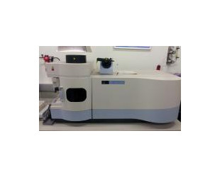
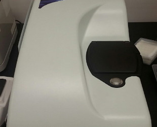
- 제작사명(모델명)Jeol (JSM-7100F)
- 구축일자2015년 10월 22일
- 사용용도시험
- 표준분류광학/전자영상장비 > 현미경 > 주사전자현미경
- 설치장소인천광역시 연수구 갯벌로 156 (송도동) F1 110-A
- 장비설명Specifications 1. Performance 1) Resolution For High Resolution condition: 1.2nm guaranteed at 30 kV or better 2.0nm guaranteed at 1 kV or better For analytical condition: 3.0nm guaranteed at 15 kV, WD 10mm, 5nA or better Gentle beam Mode: Built-in 2) Magnification : x10 to x1,000,000 or wider Magnification preset : User can be switch instantaneously from any magnification to any preset magnification. 3) Image modes : SEI, BEI 2. Electron Optical System 1) Accelerating voltage : 0.2 to 30 kV or berrer 2) Electron Gun: ZrO/W(100)Shottky type Filament Built-in 3) Gun Bias Auto and Manual mode. 4) Probe current : Up to 2 x 10⁻⁷A at 15kV or better 5) Alignment : Mechanical and electromagnetic deflection (Mechanical alignment by user can not be required)
- 구성 및 성능Features 1. High resolution field emission scanning electron microscope which schottky type FEG for the electron source should be permited 1.2nm guaranteed resolution at 30 KV and 2.0nm guaranteed resolution at 1KV and 3.0nm guaranteed analytical condition resolution or better. 2. The Schottky type Field Emission Electron Gun for the electron source should be employed to display high resolution image and analytical functions. 3. The electron beam probe current should be irradiated to analyze small area from the order 1 x 10-12A order to 2 x 10⁻⁷A. 4. The Specimen chamber is designed to introduce a large specimen of 100mm diameter and 40mm Height sample through the Airlock Chamber and also it is designed to enable various analytical devices such as EDS, WDS, EBSD, E-Beam litho. system and Backscattered electron detector. 5. For high-resolution observations, employ the GB(Gentlebeam) mode that effectively suppresses charging in non-conductive specimens such as insulating materials (ceramics, etc.) and semicondu
- 사용/활용예해당 장비는 아래와 같은 분야에 활용될 수 있다.
-주사전자현미경 기반 미세조직분석
-결정립도 정량파악
-조직 내 결정구조 분포
-Mis-orientation Angle 분포
결정상(Crystal Phase) 분산도
